I picked up some printer heads for an Okidata LED printer and checked them out under the microscope.
This ebay auction shows what the complete head looks like. An LED printer is basically a laser printer, except that instead of scanning a laser beam across the page to make the toner stick to the page, an array of LEDs does the work.
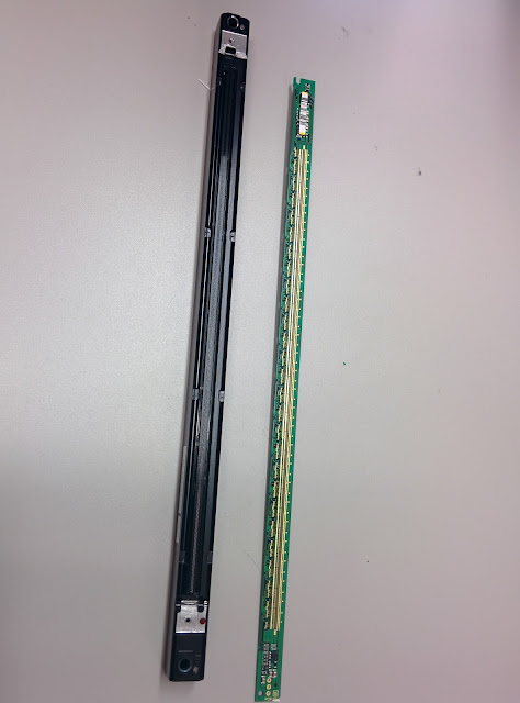
Here's the lens assembly and LED array removed from the housing:
The lens assembly has two staggered rows of lenslets. The head has some sort of tilt arrangement that I suspect they use to vibrate the lens assembly back and forth and then power the LEDs when the lenses are in the desired position. (But don't quote me on that).
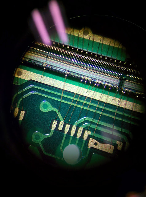
Putting the LED array under the microscope, we can see where the PCB is wire bonded to the LED driver circuitry. Normally wirebonding is used inside a chip to go from the wafer to the pins, and then the whole chip is sealed up in plastic or ceramic. But here the tiny gold wires are exposed, making them very easy to damage (which I did when removing the board from the head).

Below is a closeup. The wires at the top are all going to a common trace on the upper part of the PCB. The wires at the bottom are address/control lines going to the green/purple wafers. At first I thought this was the LED array, but it's just the control circuitry. That wafer is then wirebonded to the actual LED array, which just looks like a black line with dark gray squares between the top and middle rows of wires.
So you can see they had to run a wire for each and every LED in the array, and they're too densely packed to be able to run the wires to pads on the PCB, so instead they go wafer to wafer. Then they just need to run control lines out to the PCB so it can tell the control wafer which LEDs to turn on.


